Mastering Circuit Design: A Comprehensive Guide to Designing and Simulating Electronic Circuits with EDA Tools
Understanding Circuit Design Basics
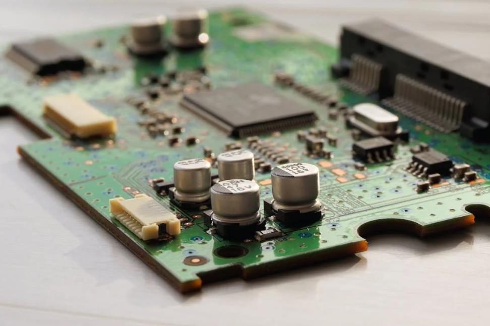
Before diving into the specifics of EDA tools, it’s important to grasp the core principles of circuit design. At its essence, circuit design involves creating schematics that represent the electronic components and their connections. These schematics are then translated into physical layouts, which are used to manufacture the actual circuits on a printed circuit board (PCB).
- Component Selection: Every circuit begins with selecting appropriate components such as resistors, capacitors, transistors, and integrated circuits. Understanding each component’s role and how they interact within a circuit is crucial.
- Schematic Design: The schematic diagram is a symbolic representation of the circuit. It illustrates how components are connected electrically and is the blueprint from which the physical PCB layout will be developed.
- Simulation: Before building the physical circuit, it’s vital to simulate it. Simulation helps verify that the circuit performs as intended and identifies potential issues, such as timing problems or signal integrity concerns.
- PCB Layout: After confirming the design through simulation, the next step is to create a PCB layout. This involves placing components on a board and routing electrical connections. The layout must adhere to manufacturing constraints and design rules to ensure reliability.
EDA Tools: Revolutionizing Circuit Design
Electronic Design Automation (EDA) tools have revolutionized circuit design by automating many of the complex and time-consuming tasks involved. These tools offer a range of functionalities, from schematic capture to simulation and PCB layout.
- Schematic Capture: EDA tools facilitate the creation of schematic diagrams with ease. Software such as KiCad, Eagle, and Altium Designer provide intuitive graphical interfaces for placing components and drawing connections. Advanced tools often include libraries of pre-defined components, making it easier to select and use standard parts.
- Simulation: One of the most powerful features of EDA tools is the ability to simulate circuit behavior. Tools like SPICE (Simulation Program with Integrated Circuit Emphasis) are integrated into many EDA platforms, allowing users to model how their circuits will behave under various conditions. This step is crucial for validating circuit performance and ensuring that it meets design specifications.
- PCB Layout: Once the schematic is complete and validated, the next phase is PCB layout. EDA tools provide capabilities to convert schematic diagrams into PCB designs. Features like auto-routing, design rule checks (DRC), and signal integrity analysis help streamline this process. Tools like Altium Designer and KiCad allow for the precise placement of components and the routing of traces, minimizing interference and optimizing performance.
- Design Rule Checking (DRC): EDA tools include design rule checking to ensure that the PCB layout adheres to manufacturing constraints. This includes checking for issues such as trace width, clearance, and pad sizes. DRC helps prevent common mistakes that could lead to manufacturing defects or operational failures.
- Gerber File Generation: Once the PCB design is complete, EDA tools can generate Gerber files, which are used by PCB manufacturers to produce the physical boards. These files contain detailed information about each layer of the PCB, including copper traces, drill holes, and silkscreen layers.
Best Practices for Using EDA Tools
To make the most out of EDA tools, consider the following best practices:
- Start with a Clear Design Specification: Before diving into design, define the specifications and requirements of your circuit. This will guide your component selection and design choices.
- Use Libraries and Templates: Take advantage of pre-existing libraries and templates available in EDA tools. They can save time and ensure that you are using standard, well-tested components and design practices.
- Simulate Thoroughly: Don’t skip the simulation phase. It’s an essential step to validate your design and catch potential issues early. Use different simulation scenarios to test how your circuit behaves under various conditions.
- Iterate and Refine: Circuit design is often an iterative process. Use the feedback from simulations and testing to refine your design. EDA tools make it easy to make adjustments and re-run simulations.
- Follow Design Rules: Adhere to the design rules and constraints provided by the EDA tool. This will help ensure that your PCB design is manufacturable and reliable.
- Collaborate and Share: Many EDA tools support collaboration features, allowing multiple users to work on the same design. Take advantage of these features to collaborate with colleagues or share your designs with the community for feedback.
Conclusion
Designing and simulating electronic circuits using EDA tools is a powerful and efficient way to bring your electronic ideas to life. By understanding the fundamentals of circuit design and leveraging the capabilities of EDA tools, you can create robust, reliable circuits with confidence. Whether you’re a seasoned engineer or a hobbyist just starting out, mastering these tools will enhance your ability to innovate and create cutting-edge electronic solutions.


Post Comment